Research
Atom-by-atom characterization of nanomaterials with atomic electron tomography
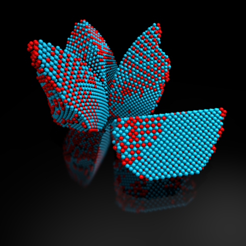 Measuring 3D atomic coordinates in materials has been a driving force behind many scientific and technological advances. Techniques such as X-ray crystallography are powerful tools to measure average atomic positions, but cannot identify individual, atomic scale defects which can strongly influence a material’s behavior, particularly in the case of nanomaterials. A single image from a high resolution electron microscope can measure crystal lattices, defects, and strain, but only in two dimensions. Extending atomic resolution electron microscopy to three dimensions via tilt axis tomography enables one to determine the 3D atomic structure of a material without averaging or using a priori information. This method has been used to isolate crystalline grains in 3D, to visualize the atomic arrangement of atoms in defects, and to localize individual atoms of a sample with 20 pm precision. From the measured atomic coordinates, 3D dislocation and strain fields can be determined and related to the surface conditions of the sample. In samples with more than one atomic species, chemical ordering can be mapped in 3D with single atom sensitivity. In this way, atomic electron tomography characterizes nanomaterials in unprecedented detail to connect local atomic structure to functionality.
Selected publications:
Closing the gap in accelerated materials discovery
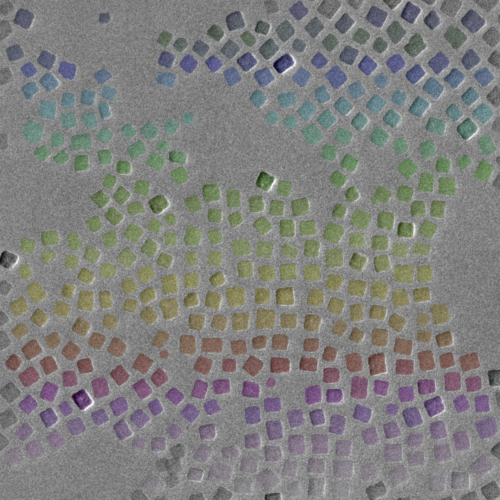 Old edisonian methods of materials discovery are quickly being replaced by high throughput screening and synthesis. However, characterization techniques have lagged behind. In order to fully incorporate electron microscopy into the process of high-throughput materials design, feedback must be given on the same timescale as screening and synthesis techniques. This project seeks to close that gap by providing an automated workflow to understanding local atomic structures. This will not only provide invaluable information for improving high throughput screening and synthesis, but will also help illuminate the role of heterogeneity in these materials. By leveraging advances in machine learning we can provide statistical information on structural properties such as shape and defect content.
Selected publications:
Atomic scale mapping of defects and interfaces in energy materials
New technologies for energy production and storage will be critical to meet the energy needs of society while mitigating the effects of climate change. As an example, solid-state lithium batteries can potentially alleviate the safety concern and electrochemical
stability issues associated with the flammable organic electrolytes used in lithium-ion batteries. High-throughput computational screening and synthesis efforts, such as the materials project, have been wildly successful in obtaining new ‘ingredients’ for solid-state batteries. However, when incorporated into devices, often these materials interact in unexpected ways at the solid electrolyte interface (SEI) upon electrochemical cycling. Characterizing the structure and chemical evolution of these interfaces and other local features at an ultrahigh spatial resolution is a critical step in designing next generation energy materials and technologies.
Many energy materials are air-sensitive and degrade quickly under the electron beam, making high resolution characterization difficult. Therefore we emphasize implementation of aberration-corrected electron microscopy, fast electron detection, scanning nanodiffraction, and a full suite of sample preparation, including air-free sample transfer. This project develops new methods to study interfaces in 2 and 3 dimensions, with the aim to incorporate advanced electron microscopy characterization into design and synthesis efforts.
Selected Publications:
Finding order amongst the disorder in non-crystalline materials
Unlike crystalline systems, amorphous materials lack long  range order. This makes their structure a mystery- although average quantities can be determined, the local structure of a disordered material has never been directly measured. This project uses advanced TEM measurements to determine local, nanometer-range order and symmetries in metallic glasses and relate them their structure.
Selected publications:
Chiral and helical nanomaterials are of interest due to their asymmetry and the varying length scales which can be tuned in these structures. These hierarchical length scales create the capability to encode complementary properties in a single nanomaterial, such as tuning catalytic and optical properties for idealized photocatalysis. Coupled optical and plasmonic properties depend on material spacing, so the ability to create interlocking and tunable morphologies of helical structures holds great promise. However, before these materials can be widely implemented in technological applications, a better understanding of the factors that govern their synthetic routes must be developed.
Here, we explore the role of defects, grain boundaries and strain in core-shell helical nanowires. Tuning the synthetic parameters results in various core-shell nanowire morphologies, including multiple-strand helices and straight nanowires with complex polycrystalline shells. We have used nanoscale and atomic-scale resolution tomography to study the structure of the AuAg core in wires of these various morphologies. Ultimately, this information can be used to better control the synthesis of these materials for tunable helical nanostructures with desired optoelectronic properties.